
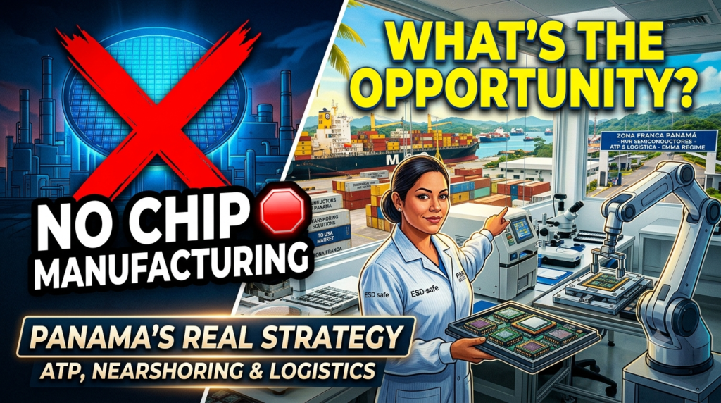
The global conversation surrounding the semiconductor industry is frequently dominated by geopolitics and sensationalist headlines. Promises of multi-billion-dollar investments and sprawling silicon megacities routinely capture official speeches. However, for business decision-makers and real capital allocation, microchips do not respond to political will; they obey a ruthless physical and economic reality.
To understand where a logistics- and service-based economy like Panama fits into this global value chain, it is essential to analyze the sector through the lens of those who have built and led global tech infrastructure. Lip-Bu Tan—industry pioneer, former CEO of Cadence Design Systems, and a central figure in the global chip ecosystem—provides a critical perspective that dismantles the myths of local manufacturing and points directly to where the real commercial opportunity lies.
1. Lip-Bu Tan’s Lessons: What the Semiconductor Industry Actually Demands
In the semiconductor industry, theory and good intentions carry zero weight without operational precision. In his strategic insights on the sector, Lip-Bu Tan highlights four operational realities that dictate any regional initiative:
A. The Fallacy of Primary Fabrication (Foundry) vs. the Urgency of Advanced Packaging
Attempting to compete in primary silicon wafer fabrication (advanced node foundries) without a pre-existing industrial base is a tactical error of astronomical proportions. A single advanced fabrication facility requires capital expenditures exceeding $20 billion, along with an ongoing consumption of natural and energy resources that is completely inaccessible to most emerging economies.
However, the primary bottleneck in modern technology is no longer simply shrinking the transistor, but how to package and interconnect multiple chips (chiplets). Lip-Bu Tan has emphasized that Advanced Packaging (ATP: Assembly, Testing, and Packaging) and geographical supply chain resilience are the exact fronts where competitiveness is decided today. A chip manufactured in Asia or North America still needs to be assembled, tested, and distributed with zero latency and maximum regulatory security.
B. Yields, Defect Density, and the Rule of Zero Margin
In the manufacturing and assembly of microchip technology, the margin for error is financially lethal. Lip-Bu Tan condenses this into critical execution metrics:
- Yield: The percentage of functional chips produced per wafer.
- Defect Density: The number of imperceptible flaws per square millimeter.
- Cycle Time: The transit speed of components through the supply chain.
A minor lapse in technical precision or a micro-outage in the global supply chain destroys operational margins. Major tech corporations are not searching for “cheap labor”; they are seeking strategic partners capable of guaranteeing zero operational downtime.
C. Execution Culture: Speed vs. Bureaucracy
Decisions within this ecosystem must be executed at “the speed of light.” State bureaucracy and endless layers of corporate committees prove fatal for a sector whose core technology becomes obsolete every 18 months. To participate in the value chain, legal, customs, and operational frameworks must operate under a startup mindset: agility, decentralized decision-making, and the total elimination of administrative friction.
D. The Specialized Talent Gap
The structural bottleneck of this sector is neither land acquisition nor tax incentives; it is human capital. Tan underscores the imperative need for specialized talent—not only in software design, but in materials science, process engineering, and applied physics. Without a workforce equipped with specialized technical judgment, physical infrastructure remains completely underutilized.
2. Panama’s Competitive Advantage: Logistics Hub and the EMMA Framework
Once Lip-Bu Tan’s thesis is understood, it becomes clear that Panama’s role is not to manufacture raw silicon, but to establish itself as the regional logistics, advanced packaging (ATP), and nearshoring distribution hub for the Americas.
       [ Global Semiconductor Supply Chain ]
                         │
     ┌───────────────────┴───────────────────┐
     ▼                                       ▼
Primary Fabrication                   Strategic Hub
  (Advanced Nodes)                (Panama's Position)
 - CapEx >$20B                     - Advanced Packaging (ATP)
 - High Energy Demand              - Supply Chain Resilience
 - Water-Intensive                 - Tax Regimes (EMMA / Free Zones)
Panama possesses unique competitive assets capable of absorbing high-value phases of the chain:
- Multimodal Logistics Connectivity: Proximity to major maritime routes and the Hub of the Americas enables the transit of high-value electronic components with minimal response times toward the North American market.
- Specialized Legal and Regulatory Regimes: Legislative frameworks such as the EMMA Law (Multinational Companies for Manufacturing-Related Services), Special Free Trade Zones, and the Special Economic Area of Panamá Pacífico provide the necessary umbrella of tax, customs, and immigration measures to establish testing centers, light assembly, and precision logistics operations.
- Geographic Resilience and Redundancy: Amid ongoing geopolitical friction among global powers, multinational enterprises are diversifying their geographic nodes to mitigate the risk of supply chain disruptions in microchip distribution.
3. The Real Execution Bottlenecks in Panama
Capitalizing on this opportunity requires strategic neutrality and a cold, objective assessment of internal deficiencies. If Panama aspires to attract serious investment in the semiconductor space, it must address three critical fronts:
- Energy Stability and Redundancy: High-tech packaging and testing facilities require uninterrupted, high-quality power flows. A single voltage flicker in the national grid can ruin entire production batches and precision calibration runs.
- Data and Utility Infrastructure: Industrial infrastructure must support clean manufacturing operations and real-time data processing without bandwidth bottlenecks in local connectivity.
- Accelerated Talent Pipeline: The local educational gap represents the primary operational brake. Immediate alignment is required between the private sector, universities, and research centers to train technicians and engineers in materials science, semiconductor logistics, and industrial quality management.
Strategic Takeaway for Business Leaders
Panama’s future in advanced technology will not be built on political promises or the illusion of competing with Asian foundry giants in wafer fabrication.
The real opportunity lies in precision logistics execution, supply chain resilience, and advanced packaging. For business leaders and capital allocators, the path forward is clear: transform geographical advantage into real operational capability, backed by robust technical infrastructure and specialized talent. Execution of a true national strategy depends entirely on interpreting these metrics correctly.
Source: LiderazgoEmpresarial.biz